הבנה בסיסית של טרמינולוגיה של מעגלים מודפסים יכולה להפוך את העבודה עם חברת ייצור מעגלים מודפסים למהירה וקלה הרבה יותר. מילון מונחים זה של מעגלים מודפסים יעזור לכם להבין כמה מהמילים הנפוצות ביותר בתעשייה. אמנם זו אינה רשימה מקיפה, אך היא משאב מצוין לעיונכם.
להיות באותו ראש עם יצרן החוזה (CM) שלך חיוני למימוש מדויק של כוונת התכנון שלך מבלי לסבול מסיבות מיותרות.עיכובים בהצעות מחיר, עיצובים מחדש ו/או סיבובים מחדש של הלוח. דיוק בתקשורת בין כל בעלי העניין בפיתוח הלוח שלך הוא המפתח.
רשימת טרמינולוגיות חשובות לתכנון PCB
טרמינולוגיה של מעגלים מודפסים
כמה מונחים מרכזיים במעגלים מודפסים מתמקדים בתיאור המבנה הפיזי של מעגל מודפס (PCB). מונחים אלה משמשים גם בתכנון וייצור, לכן חשוב ללמוד אותם תחילה.
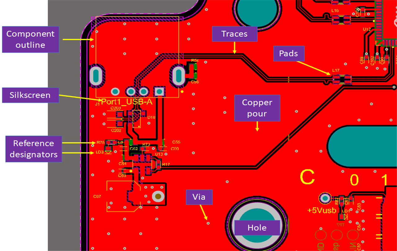
שכבות:כל מעגלי המעגל בנויים בשכבות, והשכבות נלחצות יחד ליצירתערימהכל שכבה כוללת נחושת חרוטה, היוצרת את המוליכים על פני השטח של כל שכבה.
יציקת נחושת:אזורים במעגל מודפס (PCB) המלאים באזורים גדולים של נחושת. אזורים אלה עשויים להיות בעלי צורה מוזרה.
עקבות וקווי תמסורת:מונחים אלה משמשים לסירוגין, במיוחד עבור מעגלים מודפסים מתקדמים במהירות גבוהה.
אות לעומת שכבת מישור:שכבת אותות נועדה לשאת אותות חשמליים בלבד, אך היא יכולה לכלול גם פוליגונים מנחושת המספקים הארקה או חשמל. שכבות מישוריות נועדו להיות מישורים שלמים ללא אותות.
ויאסים:אלו הם חורים קטנים שנקדחו במעגל מודפס המאפשרים לזוז קטע בין שתי שכבות.
רכיבים:מתייחס לכל חלק המונח על גבי לוח מודפס (PCB), כולל רכיבים בסיסיים כמו נגדים, מחברים, מעגלים משולבים ועוד. ניתן להרכיב רכיבים על ידי הלחמה לפני השטח (רכיבי SMD) או באמצעות חוטים המולחמים לחורי נחושת (רכיבי חורים עוברים) על גבי לוח המודפס.
רפידות וחורים:שניהם משמשים להרכבת רכיבים ללוח המעגלים ומשמשים כמיקום להחלת הלחמה.
הדפס משי:זהו הטקסט והלוגואים המודפסים על פני השטח של לוח מעגל מודפס (PCB). הוא מכיל מידע על קווי מתאר של רכיבים, לוגואים של חברות או מספרי חלקים, סמני ייחוס, או כל מידע אחר הדרוש לייצור, הרכבה ושימוש קבוע.
סמני ייחוס:אלה אומרים למתכנן ולמרכיב אילו רכיבים ממוקמים במקומות שונים על גבי לוח המעגלים. לכל רכיב יש סמן ייחוס, וניתן למצוא את הסמנים הללו בקבצי התכנון בתוכנת ה-ECAD שלכם.
מסכת הלחמה:זוהי השכבה העליונה ביותר בלוח המעגלים המודפס (PCB) המעניקה ללוח את צבעו האופייני (בדרך כלל ירוק).
זמן פרסום: 14 בפברואר 2023